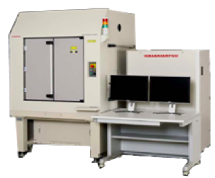
The PHEMOS-1000 is a high-resolution emission microscope that pinpoints failure locations in semiconductor devices by detecting the weak light emissions and heat emissions caused by semiconductor device defects. Since the PHEMOS-1000 is usable in combination with a general-purpose prober, you can do various analysis tasks by using the sample setups you are already familiar with. Installing an optional laser scan system allows acquiring high-resolution pattern images. Different types of detectors are available for various analysis techniques such as emission analysis, thermal analysis, and IR-OBIRCH analysis. The PHEMOS-1000 supports a wide variety of tasks and applications ranging from prober socket boards to a large-size 300 mm wafer prober.
The PHEMOS-1000 superimposes the emission image on a high-resolution pattern image to localize defect points quickly. The contrast enhancement function makes an image clearer and more detailed.
Display function
| Dimensions/Weights | Main unit: 1340 mm (W)×1200 mm (D)×2110 mm (H), Approx. 1500 kg Control rack: 880 mm (W)×820 mm (D)×1542 mm (H), Approx. 150 kg Operation desk: 1000 mm (W)×800 mm (D)×700 mm (H), Approx. 45 kg |
|---|---|
| Line voltage | AC200 V (50 Hz/60 Hz) |
| Power consumption | Approx. 1400 VA (Max. 3300 VA) |
| Vacuum | Approx. 80 kPa or more |
| Compressed air | 0.5 MPa to 0.7 MPa |
* Weight of PHEMOS-1000 main unit includes a prober or equivalent item.

Founded in 1953, HAMAMATSU Photonics Co., Ltd., is the pioneer of science and technology, coupled with the massive market share of optics science and EFA market. Hamamatsu Group's products are widely used in medical biology, high-energy physics, space exploration, precision analysis and other industries, is the optical industry leader. HAMAMATSU, with largest customer base in semiconductor and display industry, provides leading EFA solutions, OBIRCH emission microscope with high resolution location detection devices, and other professional optical products with technology patents. HAMAMATSU products are equipped with thermal, EMMI, OBIRCH functions.
Contact and consultation:http://www.spirox.com.tw/en/contact