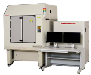
The PHEMOS-1000 is a high-resolution emission microscope that pinpoints failure locations in semiconductor devices by detecting the weak light emissions and heat emissions caused by semiconductor device defects. Since the PHEMOS-1000 is usable in combination with a general-purpose prober, you can do various analysis tasks by using the sample setups you are already familiar with. Installing an optional laser scan system allows acquiring high-resolution pattern images. Different types of detectors are available for various analysis techniques such as emission analysis, thermal analysis, and IR-OBIRCH analysis. The PHEMOS-1000 supports a wide variety of tasks and applications ranging from prober socket boards to a large-size 300 mm wafer prober.
The PHEMOS-1000 superimposes the emission image on a high-resolution pattern image to localize defect points quickly. The contrast enhancement function makes an image clearer and more detailed.
Display function
| Dimensions/Weights | Main unit: 1340 mm (W)×1200 mm (D)×2110 mm (H), Approx. 1500 kg Control rack: 880 mm (W)×820 mm (D)×1542 mm (H), Approx. 150 kg Operation desk: 1000 mm (W)×800 mm (D)×700 mm (H), Approx. 45 kg |
|---|---|
| Line voltage | AC200 V (50 Hz/60 Hz) |
| Power consumption | Approx. 1400 VA (Max. 3300 VA) |
| Vacuum | Approx. 80 kPa or more |
| Compressed air | 0.5 MPa to 0.7 MPa |
* Weight of PHEMOS-1000 main unit includes a prober or equivalent item.

日本濱松光子學株式會社(HAMAMATSU)是全球光子技術、EFA領域的領導品牌。自1953年成立以來,EFA失效分析產品銷往全球半導體各大企業,擁有數量最多的半導體業及面板業客戶。HAMAMATSU為客戶提供EFA失效分析領域的缺陷定位解決方案,開發的微光顯微鏡是業界主流的高解析度熱點定位設備,且擁有多項專利產品。設備具備Thermal,EMMI,OBIRCH等分析功能方法。