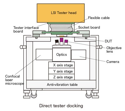
The inverted emission microscope is a backside analysis system designed to identify failure locations by detecting the light and heat emitted from the defects in semiconductor devices.
The signal detection from backside facilitates the use of probing and probe card to the wafer surface, and the sample setting can be performed smoothly. The platform, possible to mount multiple detectors and lasers, enables the selection of the optimum detector for performing various analysis methods such as light emission and heat generation analysis, IR-OBIRCH analysis, and others; moreover, letting dynamic analysis perform efficiently by tester connection.
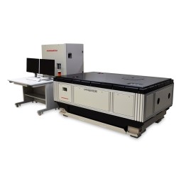
●iPHEMOS-DD
By connecting directly to the LSI tester, signal delay due to the connection cable length can be reduced, and the analysis of high-speed driving samples is possible. Direct docking dedicated prober enables multi-pin needle attachment to 300 mm wafers and with the additional option, it is possible to perform package analysis as well as pin-needle attachment by a manipulator.
The iPHEMOS-DD superimposes the emission image on a high-resolution pattern image to localize defect points quickly. The contrast enhancement function makes an image clearer and more detailed.
Display function
| Line voltage | AC 200 V (50 Hz/60 Hz) |
|---|---|
| Power consumption | Approx. 1400 VA (Max. 3300 VA) |
| Vacuum | Approx. 80 kPa or more |
| Compressed air | 0.5 MPa to 0.7 MPa |
| Dimensions/Weights | Main unit: 1980 mm (W)×1270 mm (D)×834 mm (H), Approx. 1700 kg Control rack: 880 mm (W)×700 mm (D)×1842 mm (H), Approx. 300 kg Optional desk: 1400 mm (W)×800 mm (D)×700 mm (H), Approx. 60 kg |
*Weight of iPHEMOS-DD main unit includes a prober or equivalent item.

日本濱松光子學株式會社(HAMAMATSU)是全球光子技術、EFA領域的領導品牌。自1953年成立以來,EFA失效分析產品銷往全球半導體各大企業,擁有數量最多的半導體業及面板業客戶。HAMAMATSU為客戶提供EFA失效分析領域的缺陷定位解決方案,開發的微光顯微鏡是業界主流的高解析度熱點定位設備,且擁有多項專利產品。設備具備Thermal,EMMI,OBIRCH等分析功能方法。