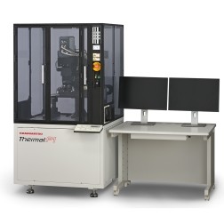
The "Thermal F1" is the next generation in thermal emission microscopy. Completely redesigned from the ground up by the same engineers responsible for the PHEMOS, the F1 features an automated microscope stage, best-in-class sensitivity, high frame rate lock-in thermography, and the ability to cover a wide range of devices from die-level to board-level fault isolation.
High sensitivity
Custom designed low-noise InSb camera with thermal lock-in achieves world class sensitivity
Covering the ideal thermal emission range from 3.7 μm to 5.2 μm, the Stirling cooled thermal emission camera seamlessly integrates with a lock-in amplifier to reduce noise and pinpoint thermal emissions.
Automated stitching function allows for board-level field of view (FOV)
Designed with ease-of-use in mind, the automated microscope stage movement combines with software image stitching function to cover an area much larger than is possible with a single objective lens.
Flexible selection of sample stage
A large area accommodating many probing stage form factors allows users to choose a stage with the best work flow and probing set-up for each labs' custom needs.
| Line voltage | AC200 V to 240 V ±10 % (50 Hz/60 Hz) |
|---|---|
| Vacuum | More than 80 kPa (Tube with outer diameter 6 mm) for prober |
| Compressed air | 0.5 MPa to 0.7 MPa (Tube with outer diameter 6 mm) |
| Dimension and weight(Main unit) | 960 mm×980 mm×1800 mm, Approx. 500 kg |
| Dimension and weight(Operation PC desk) | 1000 mm×800 mm×700 mm, Approx. 60 kg |

日本濱松光子學株式會社(HAMAMATSU)是全球光子技術、EFA領域的領導品牌。自1953年成立以來,EFA失效分析產品銷往全球半導體各大企業,擁有數量最多的半導體業及面板業客戶。HAMAMATSU為客戶提供EFA失效分析領域的缺陷定位解決方案,開發的微光顯微鏡是業界主流的高解析度熱點定位設備,且擁有多項專利產品。設備具備Thermal,EMMI,OBIRCH等分析功能方法。