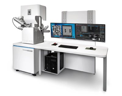
TESCAN SOLARIS is a turn-key FIB-SEM solution for the fabrication of nanostructures and nanotechnology-inspired microscale functional devices. TESCAN SOLARIS combines the most precise Focused Ion Beam with UHR-SEM featuring TriLens™ immersion optics, to ensure the best possible connection between ion beam milling and ultra-high-resolution SEM imaging. Powerful TESCAN Essence™ software allows users to customize the GUI for specific applicationworkflows and to accommodate user expertise or preferences. TESCAN SOLARIS is easy to implement in failure analysis labs and semiconductor R&D labs that assess the production quality of semiconductor devices.
|
Electron Optics
|
||
|---|---|---|
|
Electron Gun
|
High brightness Schottky emitter
|
|
|
Electron Optics
|
Triglav™ column
|
|
|
Resolution
|
Standard mode
|
0.6 nm at 15 keV
1.2 nm at 1 keV
|
|
Beam Deceleration mode
|
0.9 nm at 1 keV
|
|
|
STEM
|
0.5 nm at 30 keV
|
|
|
Maximum Field of View
|
>10 mm at max. WD
|
|
|
Electron Beam Energy
|
50 eV to 30 keV
|
|
|
Probe Current
|
Up to 400 nA
|
|
|
Ion Optics
|
||
|
Ion Column
|
Orage™
|
|
|
Ion Gun
|
Gallium liquid metal ion source
|
|
|
Resolution
|
< 2.5 nm at 30 keV
|
|
|
Ion Beam Energy
|
500 eV to 30 keV
|
|
|
Probe Current
|
< 1 pA to 100 nA
|
|
|
SEM-FIB Coincidence at
|
WDSEM = 5 mm
|
|

TESCAN is a multinational company specializing in scientific instruments for micro morphology, structure and composition analysis. It is a world-renowned electronic micro instrument manufacturer. Its headquarters are located in the world's largest electron microscope manufacturing base - Brno, Czech Republic. Its products mainly include electron microscope, focused ion beam system, multi-channel holographic microscope and relevant analysis accessories and software, which are widely used in medicine, biology, biochemistry, agriculture, material science, metallurgy, chemistry, petroleum, pharmacy, semiconductor, electronic devices and other fields.