Professional semiconductor solution provider Spirox Corporation (TWSE: 3055) will participate in SEMICON China 2023 from June 29 to July 1. This year, Spirox will present the theme "Collaborative Innovation in Semiconductor, Creating a Win-Win-Win" at the Shanghai New International Expo Center, Hall E7 (Booth No.: E7223). In addition to showcasing advanced packaging, testing, and third-generation semiconductor testing and analysis solutions spanning the entire semiconductor front and back-end processes, Spirox will also collaborate with our partner, the globally renowned electronic microscopy instrument manufacturer TESCAN from the Czech Republic, to exhibit the latest FIB-SEM and STEM technologies and semiconductor solutions at the venue.
Charles Lin, General Manager of Spirox Technology (Shanghai), stated, "Recently, the semiconductor industry has been facing uncertainties such as inflation and sluggish terminal demand. Faced with industry downturns, Spirox has always adhered to a customer-oriented approach. To meet the diverse applications and rapid development of the industry, we actively form alliances with major global equipment suppliers. With advanced equipment and technological solutions, we support customers in overcoming challenges in chip production. We believe that our joint presence with TESCAN at SEMICON China will not only deepen our collaboration but also showcase our product strength and advantages to customers, advancing towards a successful future of mutual benefit with our customers."
TESCAN is the world's first manufacturer to integrate plasma FIB into scanning electron microscopy (SEM). At SEMICON China 2023, TESCAN will simulate laboratory scenes and demonstrate capabilities in sample preparation, inspection, and failure analysis through application case studies and demonstrations of failure analysis tools. This includes abilities such as deep cross-sectioning for failure analysis at the packaging level and achieving the highest resolution terminal thinning, high-quality planar layer-by-layer delayering of semiconductor devices, high-quality TEM (Transmission Electron Microscopy) thin film sample preparation, as well as capabilities in sample preparation and analysis ranging from nanometer to millimeter scales. These capabilities cater to the demands in failure analysis of integrated circuits, circuit repair, ball grid arrays, silicon vias, wire bonding, display panels, and other process technologies.
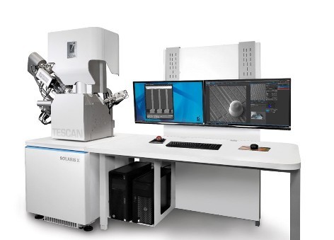
Spirox and TESCAN showcase FIB-SEM semiconductor solutions at SEMICON China 2023.
Feng Jun, General Manager of TESCAN China, explained, "The semiconductor industry is undergoing intense competition, driving the development of many high-complexity emerging technologies in the pursuit of high integration, high density, and miniaturization of chips. However, under the stringent requirements of advanced technology, higher-precision tools are preferred for development and prototype design, inspection, and failure analysis. TESCAN's scanning electron microscope (SEM) combined with focused ion beam (FIB) technology, with its high-precision analytical capabilities, is the ideal technology to meet the rapidly evolving needs of the semiconductor industry."
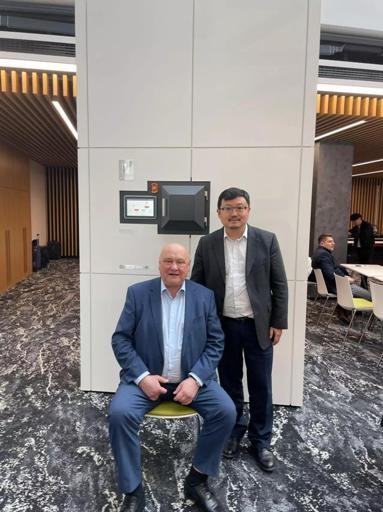
Feng Jun, General Managerof TESCAN China and Klima, Founder of TESCAN, together in front of the new TENSOR model.
In this exhibition, TESCAN not only showcases its scanning electron microscope for the first time but also presents the TESCAN Tensor model, which features excellent 4D-STEM performance, based on a 1:1 real-size replica for the first time. This allows visitors to gain a closer understanding of TESCAN's advanced technology and capabilities in scanning transmission electron microscopy. Spirox will highlight three major aspects: advanced packaging, third-generation semiconductor processes, and chip process quality assurance. Spirox will introduce high-quality solutions such as Toray Engineering's advanced wafer bonding technology, Southport's third-generation semiconductor non-destructive 3D material defect inspection and 3D stress inspection analysis services, and Hamamatsu's electrical failure analysis applications. From June 29 to July 1, feel free to visit Spirox at booth Booth E7223 in Hall E7 and meet with our experts about your application scenarios, problems, and needs.
ABout TESCAN
TESCAN provides scientific instruments for nanoscale research and analysis in the fields of earth science, materials science, life science, and semiconductor industry. For 30 years, it has been committed to developing innovative electron microscopes, micro computed tomography, and related software solutions for research and industrial customers around the world. For example, TESCAN Tensor is the first original four-dimensional scanning transmission electron microscope (4D-STEM), creating new performance and enhancing user experience. TESCAN has won a leading position in the field of micro-nano technology. TESCAN is headquartered in Brno, Czech Republic, with 13 overseas subsidiaries and more than 750 employees worldwide. For more information, please visit www.tescan.com.
About Spirox
Spirox Corporation (TWSE: 3055) is a professional semiconductor testing solution provider in the Great China. Partnered with worldwide leading suppliers, including AFORE, ERS, Hamamatsu, NI, TASMIT, SEMICS, ShibaSoku, Southport, Toray Engineering, Turbodynamics, etc., Spirox provides various integrated solutions to fulfill customer needs in testing, packaging, and inspection in semiconductor industry. Founded in 1987, Spirox is headquartered in Hsinchu, Taiwan, with additional service branches in Kaohsiung, Shanghai, Suzhou, Shenzhen, Beijing and Chengdu. For more information, please visit www.spirox.com.