Non-Distructive Defect Inspection

HOME / Services & Solutions / Compound Semiconductor Solutions / Non-Distructive Defect Inspection

【Southport】JadeSiC-NK Non-Destructive Inspection System for SiC Crystal Killer-Defects Detection

【Southport】JadeSiC-NK Non-Destructive Inspection System for SiC Crystal Killer-Defects Detection

The Best Substitution for KOH Etching Method!

  • Industry first technology for non-destructive defect inspection for SiC substrates
  • Direct insight to SiC substrates wafer mapping for killer defects distribution
  • Effective monitor the quality of SiC substrates
  • Significant costs reduction comparing to KOH etching by avoid etching SiC substrates


【Features】

  • Detect and identify defects on the surface and inside of SiC substrates with advanced NLO (non-linear optics) technology.
  • Non-destructive inspection to replace costly KOH etching method.
  • Whole SiC wafer defect scanning ability provides more accurate defect density distribution over the sampling interpolation of KOH etching method.
  • Focus on killer defects (BPD, TSD, MicroPipe, Stacking Fault) detection for SiC substrates.
  • Support 2”, 4”, 6”, 8” SiC substrates inspection.
  • Optional function of MicroArea 3D scan available.


【Advantages】

  • Effective inspection and analysis tool to improve wafer process yield and significantly reduce direct and indirect production costs.
  • No costly SiC substrate wasted, free of toxic, corrosive and hazardous material.
  • JadeSiC-NK performs whole wafer scanning to more accurately present killer defect density distribution, as opposed to using traditional optical image sampling interpolation.
  • The best tool for continuous production process improvement.


【Benefits】

  • Effectively and reliably detect and identify killer crystal defects of SiC.
  • Significantly reduce direct and indirect costs, which transfer to increase SiC substrate output compared to KOH etching method
  • State-of-the-art tool for SiC substrate production process improvement
    → Low-cost DOE (Design Of Experiment)
    → 100% inspection on extracted substrates out of one ingot for detailed ingot level quality analysis.
    → Enable effective tracking and analyzing ingots made by different batch or furnace.


【Introduction Video】


【Specifications】

Model Number
SP3055A
Model Name
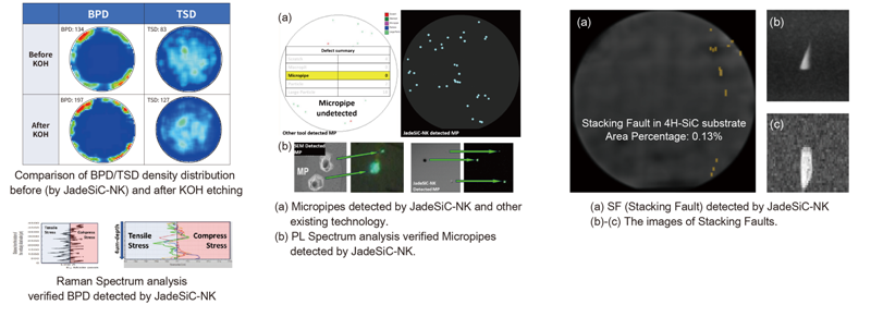
JadeSiC-NK, non-destructive inspection system for SiC killer defects (BPD/TSD/MP/SF),the best substitution for KOH etching method.
SiC Substrate /
EPI Wafer Size
2” 4” 6” 8”
Wafer Thickness
300 μm - 550 μm
Chuck
XY Stage Repeatability : 0.1 μm
Inspection Items
Whole Wafer Defect Scan (MicroPipe, BPD, TED, TSD, SF, etc.)
Whole Wafer Defect Scan
Estimated Inspection Time
1 hr   @4”wafer    
2 hrs @6” wafer
4 hrs @8” wafer
Lateral Resolution
1 μm
Analysis
MicroPipe Density (MPD)
BPD/TED/TSD Density
Stacking Fault Area Percentage
Wafer Yield
Tri-angle and Carrot**
MicroArea 3D Scan (optional)
Field of View
400 μm x 400 μm
Scanning Zoom
Yes ( 1x - 10x )
Scan Resolution
Up to 1024 x 1024
Lateral Resolution
0.4 μm
Axial Resolution
0.25 μm
Min Increment of Z stage
0.02 μm
Wide Field Module Camera
Color Camera
(FOV 400 μm x 400 μm)


Southport Co. was established in August 2014. The founding team gathered talents from cross fields such as optics, materials, physics, and information, introducing novel optical design concepts in optical engineering.Based on the two core technologies of 5D microscopy and digital optics, Southport has introduced brand-new optics concepts and technologies into four key application areas: advanced material analysis, biomedical imaging, microstructure and transparent material inspection, and digital optics. Southport is committed to focusing on solving critical problems for R&D, relieving the pains in practices for facilitating innovation. Through integrating the knowledge of light, mechanics, electronics, and software, incorporated with modular and digital design genes, and further combined with our knowledge and experiences, Southport is ready to provide the cutting-edge optical tools needed by academia and industry.