Professional semiconductor solution provider Spirox Corporation (TWSE: 3055) and the world-leading nanoscale metal probe manufacturer MesoScope Technology jointly announce the official launch of atomic force microscopy (AFM) probes. These probes, operating at the atomic scale, along with measurement technology, are designed to address obstacles in emerging process development, aiming to provide comprehensive solutions for the semiconductor measurement field.
With the rapid growth in demand for technologies such as high-speed computing, neural networks, quantum computing, and autonomous driving, the development of chip architecture technology that is low-power, small-sized, heterogeneously integrated, and features ultra-high computational speed has become a crucial industry trend and key success factor for global semiconductor manufacturers. Anticipating the future evolution of semiconductor product architectures, the continuation of Moore's Law is expected, with the transistor density per unit area continuing to grow, and the ongoing miniaturization of dimensions placing higher demands on probes. MesoScope has successfully overcome manufacturing challenges using M.S.T. (Metallic Stress Technology), pushing its products from the nanoscale to the atomic scale. MesoScope has now developed and officially mass-produced probes in up to 14 different sizes, applicable across various fields. From measuring the pads in packaging to characterizing transistor properties, MesoScope’s state-of-the-art CR1 (Curvature Radius 1nm) probes can be applied for fault analysis in processes below 2 nanometers.
Compared to other manufacturing technologies, MesoScope, with M.S.T., can shrink the size of the probe tip to the atomic level without damaging the material composition structure, allowing for a stable reduction of the probe tip size to the atomic scale and providing better resilience to the probe. When combined with the world-leading nanoprobing brand, Kleindiek Nanotechnik, this technology enables the widespread application of nanoscale electrical measurement and device characterization techniques in the research and development processes of various complex and high-speed devices, and ensures quality and reliability while reducing research and development time and the cost of device manufacturing processes to meet the significant market demand arising from the process of China's semiconductor localization.
Vincent Huang, Chairman of MesoScope, stated “In the collaboration over the past year, Spirox has demonstrated the rich industry resources and customer relationships accumulated over many years in the semiconductor industry in both Taiwan and China. The highly reliable process and quality assurance solutions Spirox provided, along with the flexible customer service quality, have been well-recognized in the industry. The development of atomic-scale probes in this collaboration represents a significant breakthrough in the global nanoprobing field. MesoScope has been dedicated to bringing cutting-edge probe products to the semiconductor industry, and believed that through the strong collaboration with Spirox, we can continue to provide high-quality solutions for the semiconductor measurement market.”
George Yang, General Manager of Spirox Technology (Shanghai), stated that MesoScope holds a world-class technological advantage in nanoprobes and nanoscale measurements. The introduction of leading-edge atomic-scale probes, along with the previous nanoprobing brand Kleindiek Nanotechnik and MesoScope’s nanoprobing measurement services, has further optimized Spirox’s product portfolio. It has enhanced the integrity of Spirox’s process quality assurance solutions. Spirox firmly believes that the collaboration with MesoScope can become a significant driver for breakthroughs and advancements in measurement for semiconductor customers in China. This partnership is expected to meet the stringent technological and measurement requirements of customers for advanced process chips, creating a win-win situation for both parties and customers.
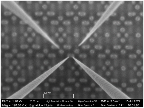
Below are two CR5A probes standing on the same contact in a 5nm process.
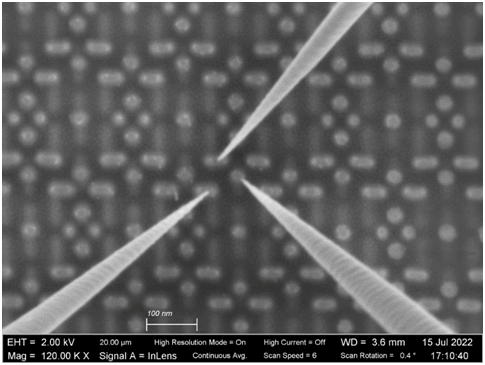
The following is the CR5A positioned on a group of transistors in a 5nm process.
MesoScope's nanoprobe sizes and corresponding analysis requirements for various processes.
|
Suitable Technology |
Model |
Curvature Radius |
Width Depth Ratio |
|
>250nm |
CR250 |
≦250nm |
1.1 |
|
>180nm |
CR200 |
≦200nm |
1.3 |
|
180nm |
CR150 |
≦150nm |
1.7 |
|
130nm |
CR100 |
≦100nm |
2.4 |
|
90nm |
CR50 |
≦50nm |
3.3 |
|
32nm/28nm |
CR35 |
≦35nm |
4 |
|
20nm/16nm |
CR20 |
≦20nm |
4.6 |
|
16nm/14nm |
CR14 |
≦14nm |
4.6 |
|
14nm/10nm |
CR10 |
≦10nm |
5.5 |
|
10nm/7nm |
CR7 |
≦7nm |
5.5 |
|
7nm/5nm |
CR5 |
≦5nm |
6.7 |
|
<3nm |
CR3 |
≦3nm |
6.7 |
|
<2nm |
CR2 |
≦2nm |
8.6 |
|
<2nm |
CR1 |
≦1nm |
8.6 |
|
<1nm |
CR7Å |
≦0.7nm |
12 |
|
<1nm |
CR5Å |
≦0.5nm |
12 |
About Spirox
Spirox Corporation (TWSE: 3055) is a professional semiconductor testing solution provider in the Great China. Partnered with worldwide leading suppliers, including AFORE, ERS, Hamamatsu, NI, TASMIT, SEMICS, ShibaSoku, Southport, Toray Engineering, Turbodynamics, etc., Spirox provides various integrated solutions to fulfill customer needs in testing, packaging, and inspection in semiconductor industry. Founded in 1987, Spirox is headquartered in Hsinchu, Taiwan, with additional service branches in Kaohsiung, Shanghai, Suzhou, Shenzhen, Beijing and Chengdu. For more information, please visit www.spirox.com.
About MesoScope
Established in Taipei in July 2006, MesoScope Technology is a world-class metal probe manufacturer and semiconductor electrical fault analysis solution provider, and has the ability to provide the most advanced nanoprobes to customers around the world.MesoScope Technology is committed to the design and development of probes and related products for typical fault analysis.For more information, please visit www.mesoscope.com.tw.