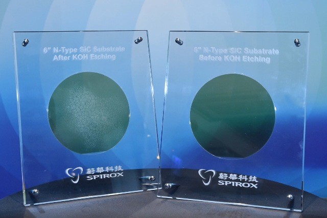
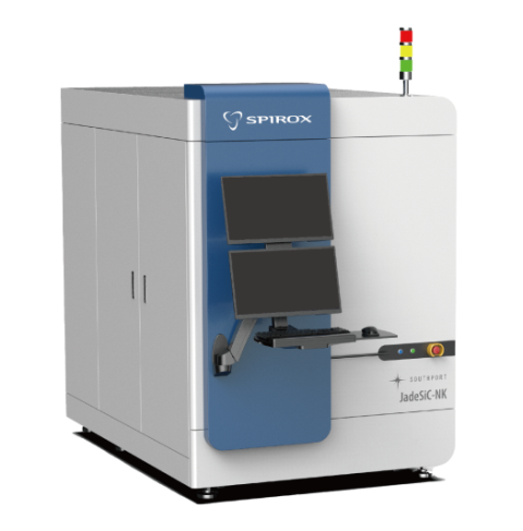
Professional semiconductor solution provider Spirox Corporation (TWSE: 3055) in collaboration with its subsidiary, Southport Corporation, has jointly launched the industry-first JadeSiC-NK non-destructive defect inspection system. JadeSiC-NK employs advanced non-linear optical technology for whole wafer scanning of SiC substrates, identifying killer defects within the substrate. It substitutes the current high-cost, destructive KOH (potassium hydroxide) etching detection method, leading to increased production yields and process improvement. Calculating based on the need to etch two substrates for each SiC ingot, JadeSiC-NK can save a substrate manufacturer with 100 crystal growth furnaces approximately 7.68 million USD in annual costs incurred due to etching losses.
In the current global trend of rising environmental sustainability awareness, many countries have set phased policy goals for electric vehicles. The demand for SiC chips is rapidly surging, especially for the production of high-temperature and high-pressure SiC power semiconductor components used in electric vehicles. The supply is far from meeting the demand.
The quality of substrate materials for compound semiconductors determines the reliability and performance of SiC chips. However, SiC crystal growth is slow, and substrate crystal defects currently can only be inspected by sampling and mathematic interpolation with the destructive KOH etching method. This makes the cost of SiC chip manufacturing processes consistently high. Major SiC substrate manufacturers worldwide are proactively investing in capacity expansion and process improvement to increase market share. If SiC substrate and component manufacturers can implement comprehensive non-destructive inspection of materials in the manufacturing process, it will not only reduce the usage of harmful chemical solutions associated with KOH etching but also allows for the early detection of defects. This, in turn, enables effective process improvement, enhances yield, and ultimately demonstrates a significant advantage in the compound semiconductor market.
General Manager of Southport, Jay Wang, states that current optical technologies in the market can only detect surface non-crystalline defects. JadeSiC-NK, however, utilizes advanced non-linear optical technology, allowing for a whole-wafer surface scan to a specific depth to provide crystal structure information, offering details on crystal defect density and distribution, and enables customers to effectively assess substrate quality to ensure the stability of the quality and performance of components produced.
Jay Wang further explains that the JadeSiC-NK non-destructive defect inspection system focuses on efficiently and stably identifying killer defects (BPD, TSD, MicroPipe, Stacking Fault). In comparison to the current KOH etching method, which involves inspecting two substrates from sliced SiC ingots, JadeSiC-NK can significantly save inspection time and substrate costs. For example, a crystal growing furnace producing four ingots per month, with JadeSiC-NK, each ingot can save the cost of two substrates (calculated at $800 per each 6-inch substrate), resulting in an estimated annual savings over $70 thousand per furnace. For a substrate manufacturer with 100 furnaces, this amounts to a annual savings of $7.68 million! Furthermore, JadeSiC-NK enables a 100% wafer inspection for the same ingot, facilitating detailed ingot analysis and batch traceability analysis which will assist customers in accelerating process and yield optimization in the high-tech compound semiconductor market.
Dr. Hao-Chung Kuo, Chair Professor of the Department of Optoelectronic Engineering at Taiwan NCYU, says that the JadeSiC-NK system launched by Spirox and Southport applies non-linear optical technology to the inspection and analysis of compound semiconductors. This innovation is expected to break through the current industry's technical bottlenecks in mass production and process improvement, providing significant impetus to the development of the industry chain. It is hoped that JadeSiC-NK, with its more effective and stable inspection technology, will establish industry standards for SiC substrate inspection, becoming a leading brand in the industry for non-linear optical technology. This, in turn, will lead continuous innovation and breakthroughs in market applications.
CEO of Spirox, Paul Yang, says “considering the instability of distribution and the pursuit of a better profit structure, Spirox has been continuously enlarging its investment in own-brand to develop solutions to fulfill customer needs. Through the acquisition of Southport, Spirox aims to accelerate the development process of our own-brand products, expanding from semiconductor packaging and testing equipment to optical inspection. The initial focus is on the highly promising defect inspection of compound semiconductor materials. This move is expected to bring about an exciting new phase for customers, employees, and investors alike.”
Paul Yang further points out that since the collaboration between Spirox and Southport in distribution, there has been a mutual understanding of mutual reinforcement. The establishment of the Advanced Opto-Material Inspection Laboratory allows the unique optical inspection technology to quickly enter industry field. Through repeated verification by customers, product specifications are adjusted to meet their needs. In addition to applying non-linear optical technology in the newly launched JadeSiC-NK, there are plans to accelerate the commercialization of advanced optical inspection technologies in areas such as MicroLED, metamaterial, silicon photonics, etc., in the future. Spirox will continue to increase research and development efforts, effectively integrating group resources to maximize synergies.
Ken Tai, Chairman of PIDA, says “it’s a great pleasure to see two Taiwanese local companies creating synergy through a mutually beneficial collaboration, generating tremendous value for the industry. The JadeSiC-NK launched by Spirox and Southport represents a groundbreaking technological breakthrough. It is not only a revolutionary product for the global compound semiconductor industry, capable of significantly reducing costs and increasing production capacity, but also showcases Taiwan's technological leadership. Spirox and Southport will play a crucial role in the future booming development of the compound semiconductor market.”
About Spirox
Spirox Corporation (TWSE: 3055) is a professional semiconductor testing solution provider in the Great China. Partnered with worldwide leading suppliers, including AFORE, ERS, Hamamatsu, NI, TASMIT, SEMICS, ShibaSoku, Southport, Toray Engineering, Turbodynamics, etc., Spirox provides various integrated solutions to fulfill customer needs in testing, packaging, and inspection in semiconductor industry. Founded in 1987, Spirox is headquartered in Hsinchu, Taiwan, with additional service branches in Kaohsiung, Shanghai, Suzhou, Shenzhen, Beijing and Chengdu. For more information, please visit www.spirox.com.
About Southport
Southport Co. was established in August 2014. The founding team gathered talents from cross fields such as optics, materials, physics, and information, introducing state of the art optical design concepts in optical engineering. Southport is founded on the two core technologies of 5D microscopy and digital optics, Southport has introduced brand-new optics concepts and technologies into four key application areas: advanced material analysis, biomedical imaging, microstructure material inspection, and digital optics. For more information, please visit the company's official website at www.southport.com.tw.