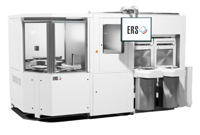
The ERS ADM System is designed for fully automated separation of wafer and carrier related to the FOWLP technology ("debonding"). Automated debonding for thermal release bonding agents is performed. After that, a proprietary thermal process is applied to reduce and control warpage of the debonded, reconstituted wafer. The system provides high throughput and repeatability of results with respect to the quality of the debonded wafer. The integrated laser scribing chamber in the ADM makes 100% monitoring of production-relevant data downstream of the debonding process possible.
It is equipped for continuous operation with optional FOUP unloading for 200 (ADM200), 300mm or 330mm (ADM330) FOWLP wafers. The system is equipped with OCR/BCR capabilities and ready for SECS/GEM interface integration. The system reads the ID on the carrier and can pass this ID number on to the factory server via the SECS/GEM interface. A recipe download from the server is then possible as is the uploading of result data to the server. Uploading of data from the automatic debonding, automatic de-taping, automatic wafer scribing (and ID-read checking) as well as data from the highly accurate warpage inspection station is possible. Immediate carrier reuse is possible.
|
ADM 330
|
|
|---|---|
|
Wafer Size
|
|
|
Handling System
|
One 3 and one 4-Axis Robot; special endeffector
|
|
Debond System
|
Thermal, force controlled
|
|
Detape System
|
Vacuum and mechanical
|
|
Detape Angle
|
Adjustable within 45°
|
|
Maximum Input Warpage
|
± 5mm
|
|
Warpage Adjust Method
|
ERS TriTemp Slide
|
|
Typical Output Warpage
|
< 500µm
|
|
UPH
|
Up to 25 depending on product
|
|
Temperature Control
|
DC PID and ERS AirCool® components
|
|
Temperature Range
|
Room temperature to +240°C (depending on station)
|
|
Debond Force
|
Adjustable
|
|
Laser Marking
|
Diode-pumped system, 1064 nm
|
|
Oxygen Free Environment
|
Optional
|
|
W x D x H
|
3126mm x 1856mm x 2105mm
|
|
Weight
|
2200kg
|

ERS electronic GmbH, based in Munich, has been producing innovative thermal test solutions for the semiconductor industry for 50 years. Today, thermal chuck systems developed by ERS in its product families; AC3, AirCool©, AirCool© Plus and PowerSense© are an integral component in all larger-sized wafer probers across the semiconductor industry. ERS also developed eWLB series for warpage adjustment, and has kept making technology progress and improvements over a decade.