|
Model Number
|
ML7000
|
|
|---|---|---|
|
Model Name
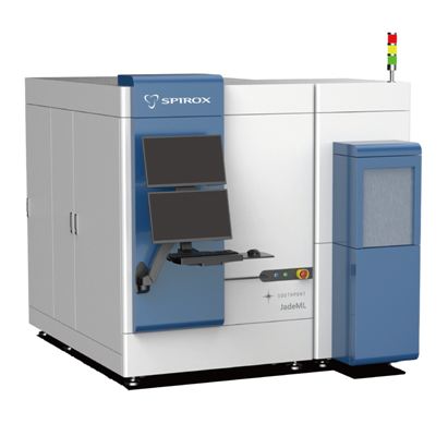
|
JadeML
|
|
|
R, G, B MicroLED Chip
on Wafer |
2" 4" 6"
|
|
|
Inspection Items
|
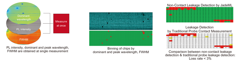
Whole Wafer PL Scan
|
PL Intensity
PL Wavelength
PL FWHM PL Dominant Wavelength
|
|
Non-contact Whole Wafer Leakage Chip Detection
|
||
|
Spatial Resolution
|
Standard Mode
(MicroLED Chip > 20 µm) |
2 µm / pixel
|
|
High Resolution Mode
(MicroLED Chip 5 - 20 µm) |
1 µm / pixel
|
|
|
Spectral Resolution
|
1 nm
|
|
|
Measurement Time
(@4” Wafer) |
Standard Mode
|
PL Scan:7.5 mins
Leakage Detection:15 mins
|
|
High Resolution Mode
|
PL Scan:30 mins
Leakage Detection:60 mins
|
|

Southport Co. was established in August 2014. The founding team gathered talents from cross fields such as optics, materials, physics, and information, introducing novel optical design concepts in optical engineering.Based on the two core technologies of 5D microscopy and digital optics, Southport has introduced brand-new optics concepts and technologies into four key application areas: advanced material analysis, biomedical imaging, microstructure and transparent material inspection, and digital optics. Southport is committed to focusing on solving critical problems for R&D, relieving the pains in practices for facilitating innovation. Through integrating the knowledge of light, mechanics, electronics, and software, incorporated with modular and digital design genes, and further combined with our knowledge and experiences, Southport is ready to provide the cutting-edge optical tools needed by academia and industry.