- ROI (Region of Interest) inspection modes
- Script scanning workflow
- Coordinate-based inspection mode
- Random inspection mode
Non-Destructive TSV Inspection System
● Exclusive optical scanning technology with patented non-destructive defect inspection enables real-time analysis without making physical cross sections.
● AI-assisted precision inspection of TSV side walls ensures accurate defect detection, supporting both blind and through vias.
● Individual via TSV depth and diameter measurement, combined with fast zone-based IPQC sampling, delivers rapid, quantified wafer-level insight for confident die qualification and classification.
PRODUCT DESCRIPTION
PRODUCT DESCRIPTION
FEATURES
FEATURES
-
TSV Inner Wall Defect Inspection
Defects like striations, scallops, and cracks can damage the insulation layer and cause leakage currents. -
Defect Data Collection and AI Database
Systematically collect and organize defect datasets; leverage AI to build an intelligent database that enables quantitative analysis, optimizes process parameters, and improves yield and manufacturing efficiency. -
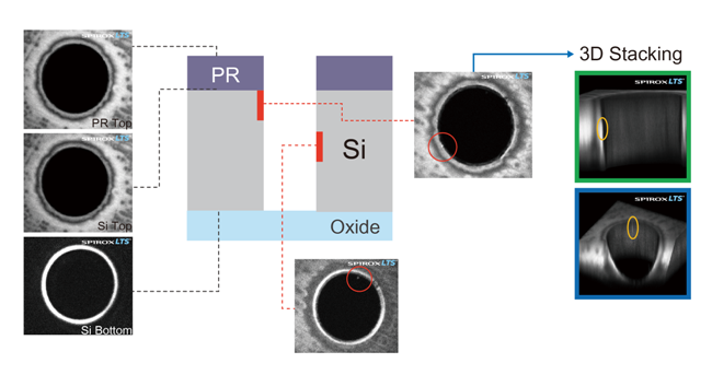
From Individual TSV Geometry to Full-Wafer Statistics
Fast IPQC sampling enables data-driven die qualification.
Multi-Mode Automatic Inspection with Flexibility
AI-Assisted Detection for TSV Defect Identification
Intuitive User Interface
Automated Loading and Unloading
ADVANTAGES
ADVANTAGES
Non-Destructive Inspection
Non-linear optical inspection and patented SpiroxLTS® technology enables precise, quantitative defect evaluation without sample destruction.
Quick Sample Inspection
SP8000S offers a faster and more efficient inspection process compared to traditional cross-sectional scanning electron microscopy (SEM).
Per-Via TSV Measurement & Fast IPQC
Delivers rapid, quantified wafer-level insights by measuring individual TSV depth and diameter, while enabling zone-based IPQC sampling for efficient die qualification and classification.
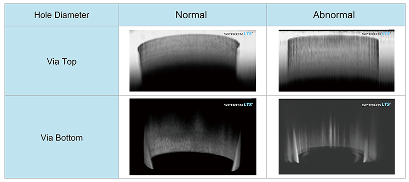
3D Imaging Comparison of TSV Quality
FUNCTION DESCRIPTION
FUNCTION DESCRIPTION
Improving Efficiency and Yield:
Online automated inspection with big data collection reduces SEM sampling, accelerates process optimization, and significantly improves product quality and yield.
Online automated inspection with big data collection reduces SEM sampling, accelerates process optimization, and significantly improves product quality and yield.
Reducing Production Costs:
Reducing defect rates and rework times, thus lowering material waste and production costs.
Reducing defect rates and rework times, thus lowering material waste and production costs.
Enhancing Process Optimization:
Using AI analysis to continuously optimize processes, improving stability and performance.
Using AI analysis to continuously optimize processes, improving stability and performance.
Increasing Market Competitiveness:
Enhancing product reliability and consistency, attracting more customers and collaboration opportunities.
Enhancing product reliability and consistency, attracting more customers and collaboration opportunities.
Data-Driven Decision Making:
Providing precise data analysis to optimize process parameters, enabling quick response to market changes and customer demands.
Providing precise data analysis to optimize process parameters, enabling quick response to market changes and customer demands.
-
Capturing TSV Striation Cross-Section and 3D Imaging
-
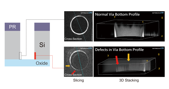
Bottom TSV Striation Cross-Section and 3D Imaging
PRODUCT SPECIFICATIONS
PRODUCT SPECIFICATIONS
| Item | Content | |
|---|---|---|
| Model Number | SP8000S | |
| Model Name | Non-Destructive TSV Inspection System | |
| Key Optical Technology | SpiroxLTS® Nonlinear Optical Inspection | |
| Applicable Sample Size | 12”/ 8” Wafers | |
| Load / Unload | Automated Loading and Unloading | |
| Application & Inspection Items |
Non-Destructive TSV In-Line Inspection System (IPQC) Designed for non-destructive quality inspection of TSV structures on function wafers. It is applied for sampling inspection during the mass production stage to monitor process stability in real time, improving overall yield and efficiency. The system features real-time inspection of via wall defects and detection of TSV bottom oxide residue.
|
Stability Verification for TSV Etching Equipment Designed to verify the stability of TSV etching equipment, enabling nondestructive measurement of TSV depth and real-time inspection of via wall defects.
|
| Objective Magnification | 20x / 40x | |
| FOV/Measurement Time | Point Scanning: FOV 400 μm x 400 μm;3.5 seconds / frame ; 100 frames ≒ 6 minutes | |
| Measurement Mode | Micro-area imaging, zone-based automatic measurement, and coordinate-based measurement; user-defined scanning sequences are also available. | |
| Measurement Resolution | Image Minimum Resolution 0.5 μm | |
| Motion Resolution | X-Y axis Motion Resolution 0.1 μm;Z axis Motion Resolution 0.1 μm | |
| Air Supply |
|
|
| Options | Opt. 001: Transmissive Single Optical Path;Opt. 002: Transmissive Dual Optical Path;Opt. NLR: Remove Automatic Loader/Unloader | |
| Dimensions/Weight | Length 2.795 m x Width 1.830 m x Height 1.900 m Weight 2750 kg | |
| Electrical Specification | 220V 60Hz AC 3500W | |
| Inspection Image |
TSV Sidewall Inspection 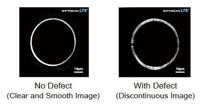 TSV Bottom Oxide Residue Detection 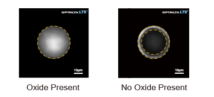 |
TSV Via Depth (CD=5 μm) Measurement Example: Statistical data of the 9 shots for the whole wafer
 |